Intel says it has processed over one million High‑NA EUV wafers, approaching worldwide total
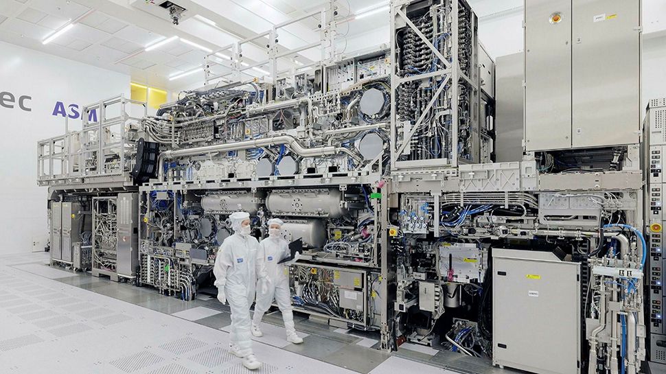
Intel announced it has processed more than one million wafers using High‑Numerical Aperture (High‑NA) extreme ultraviolet (EUV) lithography tools, a milestone that puts the company near the global output of this cutting‑edge technology.
High‑NA EUV, the newest generation of lithography equipment, enables chip makers to print finer circuit features than ever before, supporting the move to 3‑nanometer and smaller process nodes. The machines are supplied exclusively by ASML, a Dutch firm whose technology is considered the bottleneck for advanced semiconductor manufacturing.
Intel says the million‑wafer tally aggregates all activity on the new scanners, from tool qualification and research‑and‑development runs to full‑scale production. The figure reflects the company’s accelerated rollout of High‑NA EUV across its newest fabs, including the recently opened facilities in Arizona and Ohio that are geared toward high‑performance computing and artificial‑intelligence workloads.
ASML reports that a total of 1.35 million High‑NA EUV wafers have been processed worldwide to date, meaning Intel’s count represents roughly three‑quarters of the global volume. The remaining quarter is split among a handful of rivals, chiefly Taiwan’s TSMC and South Korea’s Samsung, both of which are also expanding their High‑NA capacities but at a slower pace.
The milestone carries strategic weight for Intel, which has been working to close the technology gap with TSMC and Samsung. By securing a dominant share of High‑NA throughput, Intel aims to strengthen the U.S. semiconductor supply chain, a priority underscored by recent government initiatives to boost domestic chip production.
Looking ahead, Intel says it will continue to increase wafer throughput on its High‑NA tools as more lines come online and yield improvements are realized. Industry observers expect the company’s next generation of processors, slated for launch later this year, to benefit from the enhanced patterning capability, potentially narrowing the performance lead held by its Asian competitors.



Comments (0)
Be the first to comment.
Join the discussion